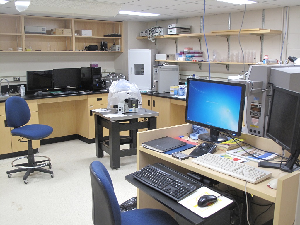
Microscopy Laboratory
About the Laboratory
- Materials characterization
- Surface characterization
- In situ cell imaging
Laboratory Contact
Location:
B9A
B9B
Phone Number:
(306) 966-1729
Laboratory Managers:
Jason Maley
George Belev
Instruments and Techniques Used In Lab
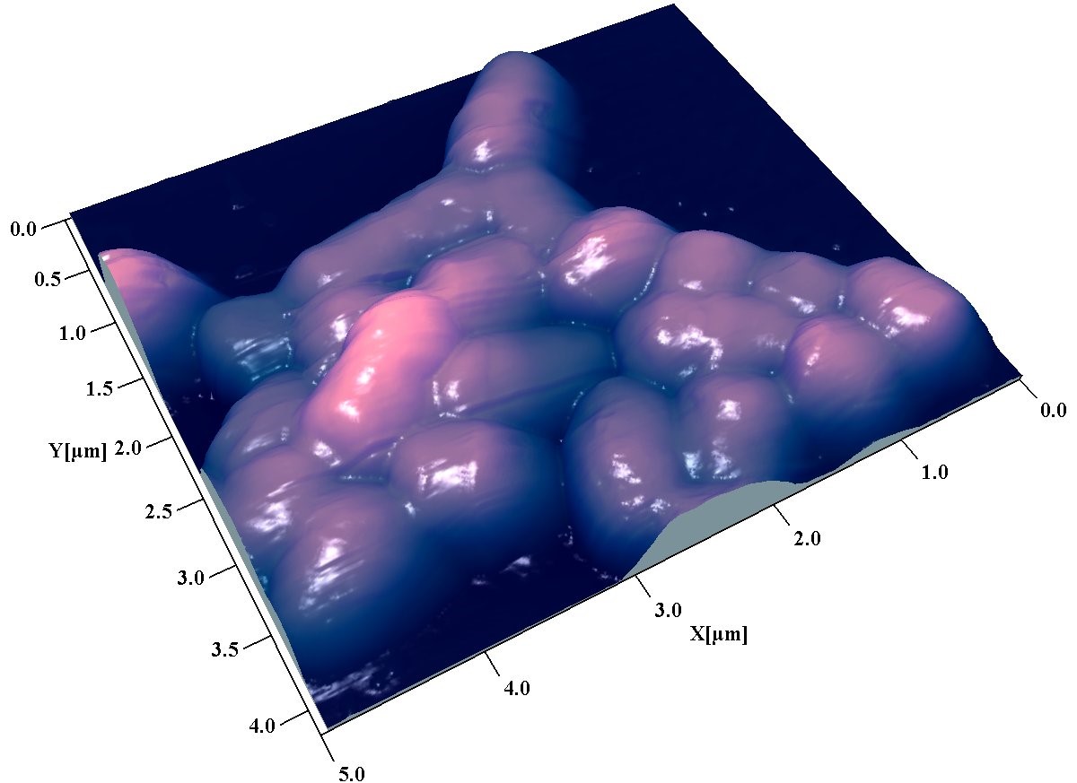
AFM is a collection of scanning probe microscopy techniques that measure various properties of materials at or near their surfaces. The AFM uses commercially available nano-sharpened probes to measure the 3D morphology as well as other physical properties of a sample under various conditions (wet, dry, temperature variation, etc.). AFM applications at the SSSC have found widespread use in engineering, agriculture, physical sciences, and health sciences research.
Selected Applications:
- Surface roughness and nano-sized surface defects, thin films
- Particle size distribution
- Protein aggregation
- Polysaccharide identification and distribution
- Tip-sample adhesion measurements
How it works:
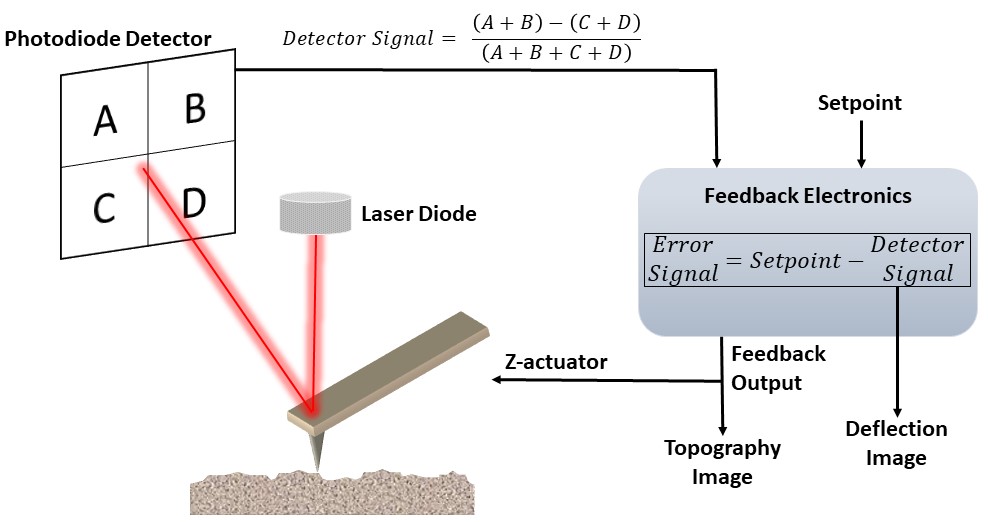
The basic setup of an AFM consists of raster-scanning a sharpened AFM probe across a surface using a calibrated XYZ-actuator (ex. Piezotube). The probe maintains a constant force (contact mode) or amplitude (intermittent contact) through the instrument’s feedback electronics. While tracking in the XY plane, the AFM “senses” changes in the z-direction by measuring the laser diode reflection from the backside of the AFM probe (detector signal). The feedback electronics will determine the error signal, which is the difference between the force/amplitude setpoint (software input) and the detector signal. The feedback electronics will apply an offset voltage to raise/lower the actuator in order to minimize the error signal. The resulting Z-feedback output signal measured at each pixel mapped is the topography image. If the feedback electronic gains are optimized (I, P gains), the deflection image will be the 1st-derivative of the topography image. Both topography and deflection images are collected simultaneously.
Instrument: Agilent 5500 AFM with MAC Mode III controller (triple lock-in amplifier)
Multipurpose Scanner: 90 µm x 90 µm Scan Range; 8 µm Z-range (0.5 Å RMS)
The SSSC has a Agilent 5500 AFM. This instrument has many capable AFM modes and accessories available, including:
- Contact AFM
- Lateral Force AFM (LFM) or Frictional Imaging
- Acoustic AC Mode (AAC) – commonly referred to as Dynamic Mode AFM
- MAC ModeTM
- Phase Imaging (AAC and MAC Mode provides simultaneous amplitude/phase imaging)
- Current Sensing AFM (CS-AFM) for conductive/semiconductive substrates
- Pulsed Force Mode (collects adhesion and stiffness maps)
- Electrochemical AFM (EC-AFM) – contact or dynamic force modes
- Temperature stages allow measurement from -30 oC to 250 oC
- Kelvin Probe Force Microscopy (KPFM)
Raman microscopy couples a standard optical microscope with a Raman spectrometer, allowing researchers to obtain “chemical” maps of their samples. The addition of an aperture within the detector path provides the confocal ability of the Raman microscope. This eliminates
Raman microscopy provides
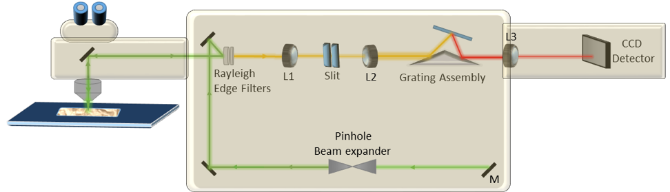
Figure 1. Confocal Raman microscopy merges a Raman spectrometer, and a confocal optical microscope to provide very high spatial resolution “chemical” mapping for researchers. The laser excitation source is guided towards the sample by mirrors (M). An optical objective focuses the laser onto the sample, and the backscattered light is mainly elastically scattered and rejected with a Rayleigh filter. A small portion of
The SSSC has 2 Renishaw Invia Reflex Raman microscopes. Raman imaging can be easily obtained and the instrument provides a few different options:
- StreamlineTM Imaging– A method unique to Renishaw in which acquires fast image acquisition using the
linescan function and collecting spectra from multiple pixels simultaneously. This method can only be run in “static” mode (gratingcentered at user selected Raman shift). - Regular Mapping – Traditional raster scanned image acquisition where each image pixel is measured. It is possible to collect full spectra in this mode, but it may be
time consuming . - Line Scan – Measure across a
user specified line - Depth Scan – Measure the depth of a
user specified line.
Typical applications include:
- Catalyst distribution on
support material - Carbon nanomaterials
- Tissue mapping
Instrument Specifications
Instrument –Renishaw Invia Reflex Raman Microscope (with FTIR)
The Renishaw Invia Reflex Microscope is equipped with an IlluminatIRII FTIR microscope accessory (Smith’s Detection, Danbury, CT), and it is the only one available in Canada. The microscope is equipped with
Instrument Specifications
|
Laser Pathway |
|
Filter Set |
Polarizers |
Grating (line/mm) |
|
514 nm Ar+ Laser ( |
Edge Filters (100 cm-1) |
z(x,x)z’, z(x,y)z’ |
1200, 1800, 2400 (special request) |
|
|
785 nm Laser Diode (Renishaw Inc.) |
Edge Filters (100 cm-1) |
z(x,x)z’, z(x,y)z’ |
1200 |
|
|
Light Microscope |
Leica DC2500M equipped with 5X (NA=0.12), 10X (NA=0.25), 20X (NA=0.40), 50X (NA=0.75), 100X (NA=0.85), 50X LWD (NA=0.40) |
|||
|
XYZ Motorized Stage |
MS20 Encoded Stage, Renishaw, UK) with 100 nm step sizes which
|
|||
Instrument –Renishaw Invia Reflex Raman Microscope (with Fiber Optic Probe)
A recent addition to the SSSC, this Renishaw Invia Reflex Microscope is equipped with an external
Instrument Specifications
|
Laser Pathway |
|
Filter Set |
Polarizers |
Grating (line/mm) |
|
514 nm Ar+ Laser ( |
Edge Filters (100 cm-1) |
z(x,x)z’, z(x,y)z’ |
1200, 1800 |
|
|
785 nm Laser Diode (Renishaw Inc.) |
Edge Filters (100 cm-1) |
z(x,x)z’, z(x,y)z’ |
1200 |
|
|
Light Microscope |
Leica DC2500M equipped with 5X (NA=0.12), 10X (NA=0.25), 20X (NA=0.40), 50X (NA=0.75), 100X (NA=0.85) |
|||
|
XYZ Motorized Stage |
MS10 Encoded Stage, Renishaw, UK) with 100 nm step sizes which
|
|||
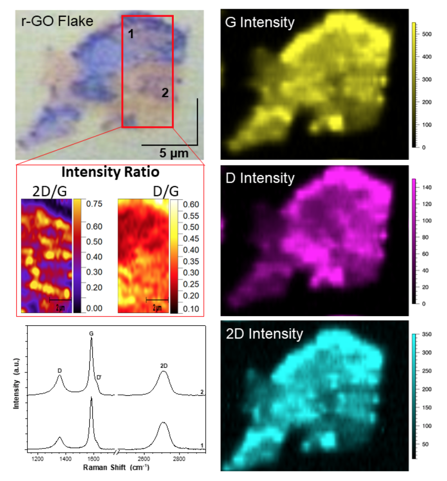
Image Caption: StreamlineTM Raman mapping (λex = 514.5 nm, 60s acquisition time) of a reduced graphene oxide (r-GO) flake deposited on Au-coated Si wafer. Raman measurements were acquired using a 100X (NA = 0.9) objective, and corresponding maps were 0.5µm x 0.5µm pixel size for a total of 2604 spectral acquisitions
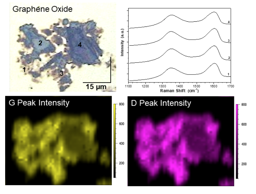
Image Caption: StreamlineTM Raman mapping (λex = 514.5 nm, 5s acquisition time) of a graphene oxide (GO flake deposited on Au-coated Si wafer. Raman measurements were acquired using a 50X (NA = 0.75) objective, and corresponding maps were 1.2µm x 1.2µm pixel size for a total of 2112 spectral acquisitions
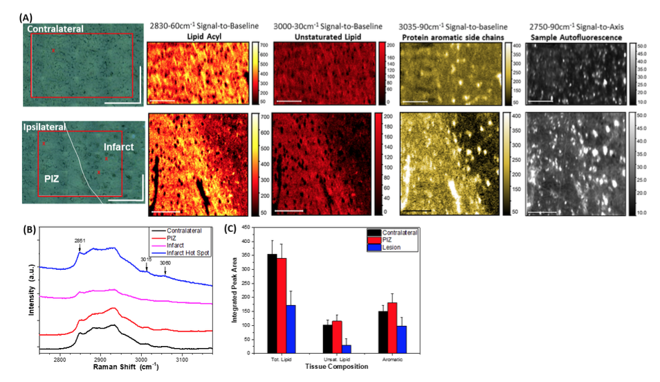
Image Caption – StreamlineTM mapping λex = 514.5 nm, 30s acquisition time) of
Field-emission scanning electron microscopy (FE-SEM) is a high-resolution imaging technique that uses
Secondary electron imaging produces a very high resolution of a sample surface because SEs are emitted from very close to the specimen surface. BSE
SEM is performed under vacuum conditions using a high energy beam of electrons, so sample charging is a concern. Specimens are mounted on a conductive substrate, and non-conductive specimens are generally sputter-coated with a conductive material (graphite, gold, etc.).
Instrumentation
Hitachi SU8010 (located and operated by our partners at the at the WCVM Imaging Centre)
The Hitachi SU8010 SEM is a semi-in-lens type cold field emission SEM that uses a small energy spread to deliver ultra-high resolution imaging capabilities. This SEM uses 2 different image capturing modes:
Beam Deceleration – The beam deceleration mode applies a negative voltage to the specimen, decelerating the primary electrons before the beam interacts with the specimen. Landing voltages can be reduced to as low as 100V with a low lens aberration. This mode provides:
- High-resolution imaging at low landing voltages
- Absolute surface information from the sample
- Less sample damage
SE-BSE Signal Mixing Function (Super ExB) – The Super ExB function expands the signal detection capability by changing the voltage of the signal conversion electrode in the objective lens, allowing the SE-BSE signal ratio to be adjusted (100 steps). This is especially useful for non-conductive samples where low energy secondary electrons show a charge up
Instrument Specifications
|
SE Detector |
|
|
SE Resolution |
1.0 nm (Vacc 15 kV, WD = 4mm) 1.3 nm (landing voltage 1 kV, WD = 1.5 mm) |
|
Upper Detector |
Available |
|
Lower Detector |
Available |
|
Specimen Stage |
||
|
Stage Control |
1.0 nm (Vacc 15 kV, WD = 4mm) 1.3 nm (landing voltage 1 kV, WD = 1.5 mm) |
|
|
Stage Transverse Range |
X |
0 ~ 50 mm |
|
Y |
0 ~ 50 mm |
|
|
R |
360° |
|
|
T |
-5° ~ 70° |
|
|
Z |
1.5 ~ 30 mm |
|
|
Maximum Sample Size |
100 mm diameter |
|
Fluorescence Lifetime Imaging (FLIM) is the measurement of the lifetime of a fluorophore in an excited electronic state as a function of position on an image. This gives a picture of environment of the fluorophore. The lifetime of a fluorophore can change with chemical composition (pH, calcium concentration) or because of quenching (FRET, oxygen). At the SSSC, FLIM is based on the time domain acquisition of information in conjunction with the laser scanning confocal microscope. The pulsed laser system can used in pico- or femtosecond mode with a variety of repetition rates, and it can be used in the visible or infrared regions.
For more detailed information, click here
Optical (light) microscopy, one of the oldest microscopy techniques, uses visible white light sources and a specialized lens to magnify samples of interest. Modern microscopes are capable of capturing contrast detail from most surfaces, and optical capacities can distinguish features in the low-µm region.
Depending on the type of samples, different illumination methods are available on most modern microscopes.
- Reflected optical microscopy – Light source passes through objective lens, and light scattered from sample is collected from objective lens and sent through oculars for viewing. Suitable for opaque samples such as metal samples, ceramics, semiconductors, thin films, etc.
- Transmitted optical microscopy – Light source passes through condenser located below sample. Light that passes through sample is collected by objective lens and oculars for viewing. Suitable for transparent specimens such as thin rock sections, single crystals, biological samples, etc.
- Polarized light microscopy – Polarizers are placed in both (1) the light path before sample, and (2) light path between objective back aperture and viewing port. This sample is suitable for birefringent materials such as single crystals,
Selected Applications
- Grain size and morphology examination
- Microstructure – amorphous and crystalline regions
- Phase identification
- Larger defects on surfaces
- Thin film cross sections
Instruments Available – Leica DM2500-P Microscope
The SSSC has a Leica 2500DM-P microscope with optical magnification of 50-1000X. All available objectives are air polarization objectives, a rotational stage, and polarization in either reflected or transmitted optical microscopy modes. A CCD camera will be available for image collection in the near future.One class of events characterizing the capability of modern electronics to operate under normal and elevated levels of ionizing radiation are the so called single event effects (SEEs). Such events appear more often at high altitude and space application, and are capable of causing wide variety of effects ranging from small glitches in the output signal to complete system failures. Under normal conditions SEEs are most likely to be caused by energetic protons and heavy ions interacting with the sensitive areas of the electronic devices and logically conventional testing for SEE sensitivity of the newly developed electronic circuits is carried out at accelerator (proton and heavy ion) facilities. However over the past 20 years pulsed femptosecond and picosecond lasers have proven to be an effective source for evaluation of SEE sensitivity of electronic devices. Such lasers provide easy spatial and temporal control over how the device under test is irradiated. The laser beam can be focused to irradiate much smaller sensitive areas compared to the case when charged particles are used for the testing. Additionally, the lasers do not cause device performance and operation degradation due to cumulative radiationdose effects, giving the flecsibility to retest the device if desired.
For more detailed information, click here
Two-photon excitation microscopy is best at reducing out-of-focus excitation, reducing the risk of bleaching a volume of the sample before the imaging process is completed. The two-photon process requires high photon density, which is achievable at the focus point of the objective with ultra-short light pulses. TPEM may reduce photo-toxicity and help to improve live cell imaging. The longer wavelength range required for the technique can make it possible to image thicker samples compared to excitation in the ultraviolet and visible ranges.
For more detailed information, click here
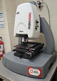
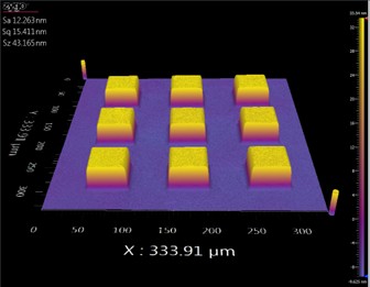
Coherence Scanning Interferometry (CSI) is an optical microscopy technique that measures the 3D metrology properties of surfaces. The Zygo CSI instrument has an interferometer contained within the microscope objective, and the short coherence length of white light causes a shallow interference depth allowing a range of smooth to rough/discontinuous surface topographies to be measured. The objective moves perpendicular to the sample and the interference signal is measured with a high speed, low noise camera. The resulting images can deliver high quality and very precise nm to sub-nm height precision for all objectives.
Instrument: Zygo Corporation NewView 8200
Objectives:
- 5X optical lens
- 75X (NA 0.08) Michaleson objective (WD = 4.5 mm; Spatial Sampling = 5.91µm)
- 50X (NA 0.55) Mirau objective (WD = 3.4 mm; Spatial Sampling = 0.33 µm)
For more detailed information, click here
Training Information
The Raman/FTIR microscope open to any academic research group. SSSC personnel will first train researchers on the instrument and offer assistance in experimental development if needed. Training typically lasts 1-2 hours. After training, researchers may use the instrument independently and reserve the instrument time through SSSC Evolution site.
Technical Resources
- Nanohub (wealth of online presentations for AFM and other nanoscience topics)
- Bruker AFM (many application notes)
- Asylum Research
- Leica Microsystems Science Portal
- Renishaw
- ThermoFisher Raman Spectroscopy Academy
- ThermoFisher FTIR Spectroscopy Academy
- LibreTexts – Infrared Absorption Table
- LibreTexts - IR Interpretation
- Hitachi HT7700 video
Data Analysis Resources
- Gwyddion (free SPM Analysis Software)
- Getting Started in Gwyddion (a series of videos)
- Renishaw Wire (available at SSSC)
Consumables
- Nanoscience Instruments (AFM Probe Store)
- NanoWorld (AFM probes)
- NT-MDT (AFM probes)
- SPI Supplies (other AFM consumables)
- Ted Pella (other AFM consumables)
- Au-Si wafers (Platypus Technologies)
- FTIR MirrIR Slides (Kevley Technologies)